Semiconductors @ Home
Prelude
This was one of my hardest projects yet, creating semiconductor devices in my garage.
In this project, I created a PN Junction diode and a transistor. I am still working on getting the transistor details written up, but for now I have information for the diode fabrication process here.
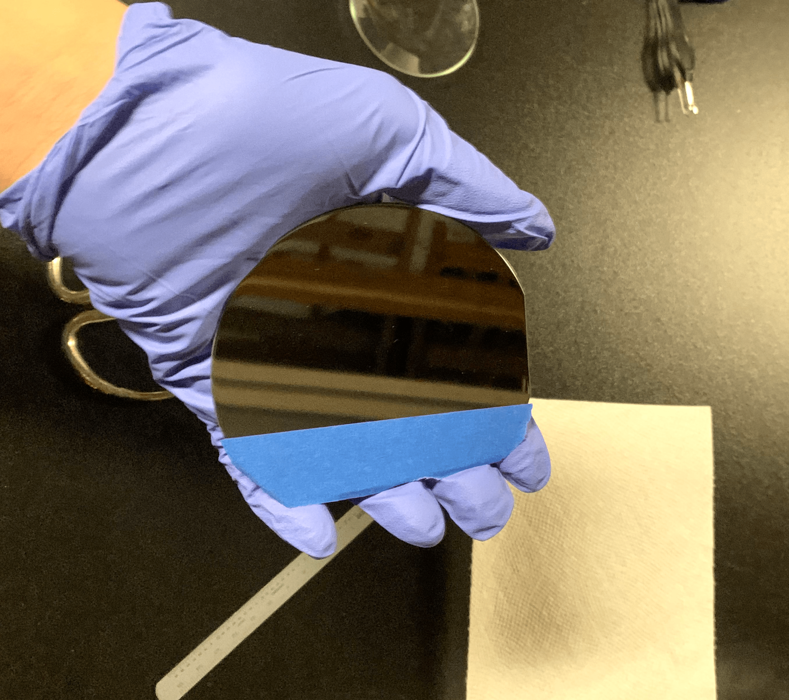
<100> P-type silicon wafer
Atomic Processes
The semiconductor fabrication process has multiple simple "atomic" steps that are repeated and done one after another to build up an entire chip.
The main ones that are used are: Oxide growth, Oxide etching, and Doping. There are others, such as the deposition of metallic layers, although I will not be covering them here, as they are significantly more complex and require more specialty equipment than I have.
Semiconductor devices are fabricated out of silicon wafers or dies. I used <100> P-type silicon wafers for this entire project. This means that my wafers were pre-doped with boron atoms to render them P-type semiconductors, and that the crystal orientation is of the <100> miller index type.
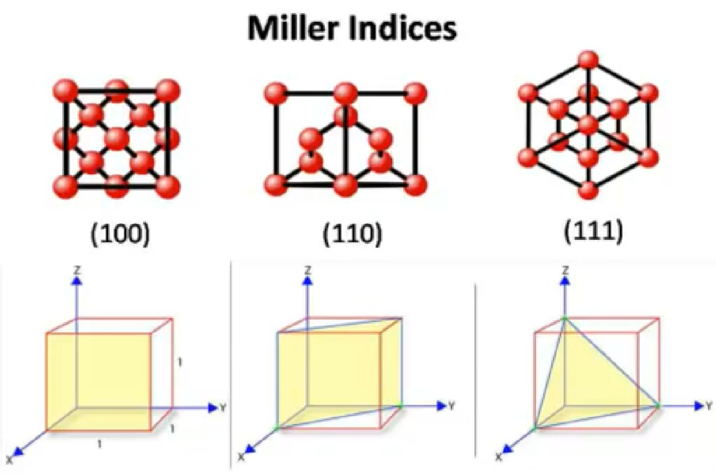
Miller indices in crystallography
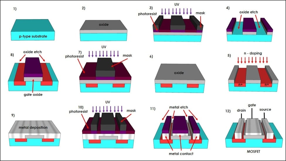
Typical semiconductor fabrication steps
Oxide Growth
Oxide growth is the step where an oxide layer is grown on the surface of the die. This oxide layer is chemically composed of Silicon Dioxide, SiO2, and is formed by the reaction of oxygen (or water) with the bare silicon surface of the die. I achieve this by heating the silicon die at 1200°C in a tube furnace for roughly 2 hours. The exact duration of time depends on the desired oxide thickness, and can be calculated using Deal-Grove oxide growth models.
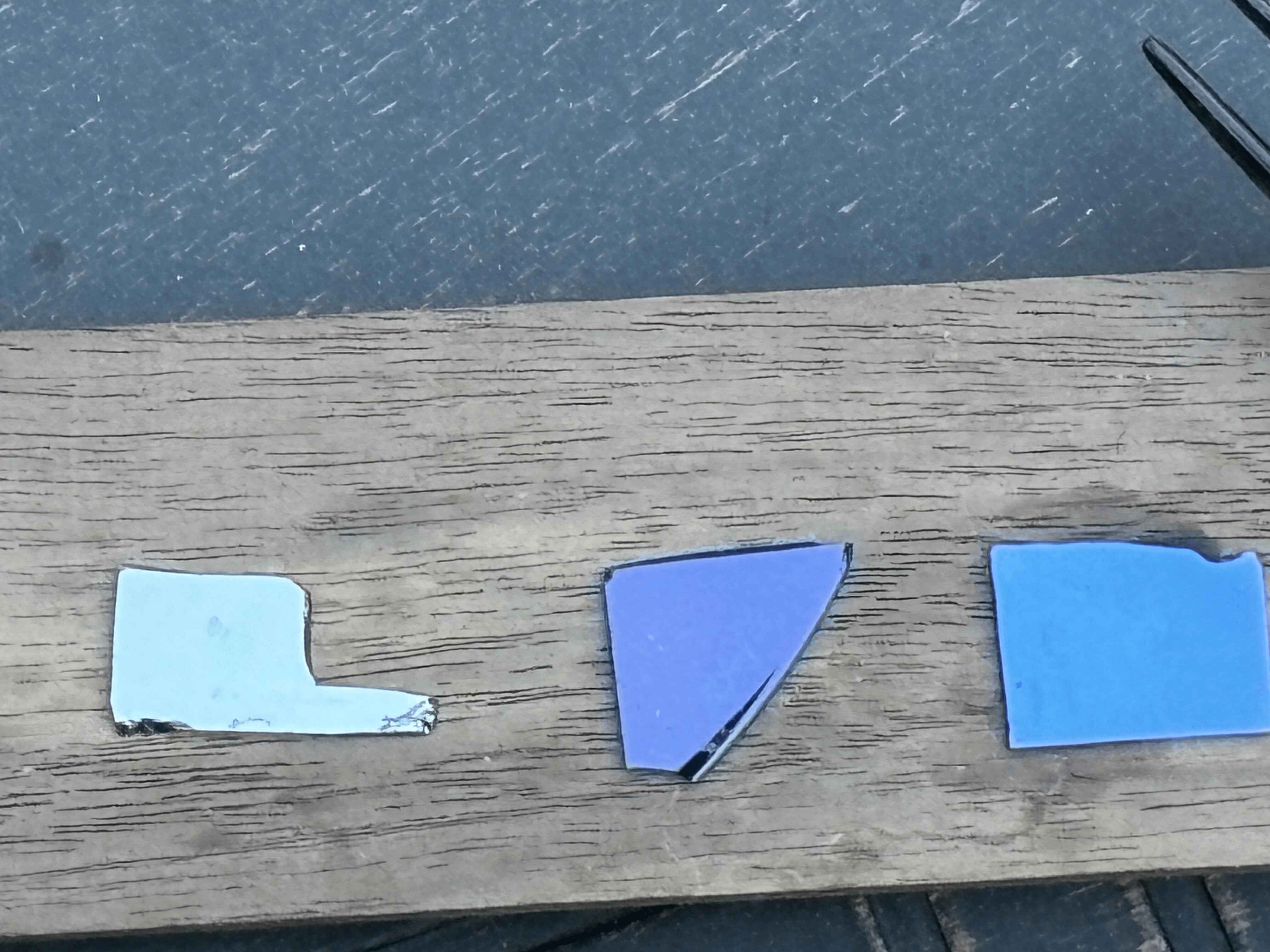
Oxide growth tests at different times yield different thicknesses, which appear as different colors
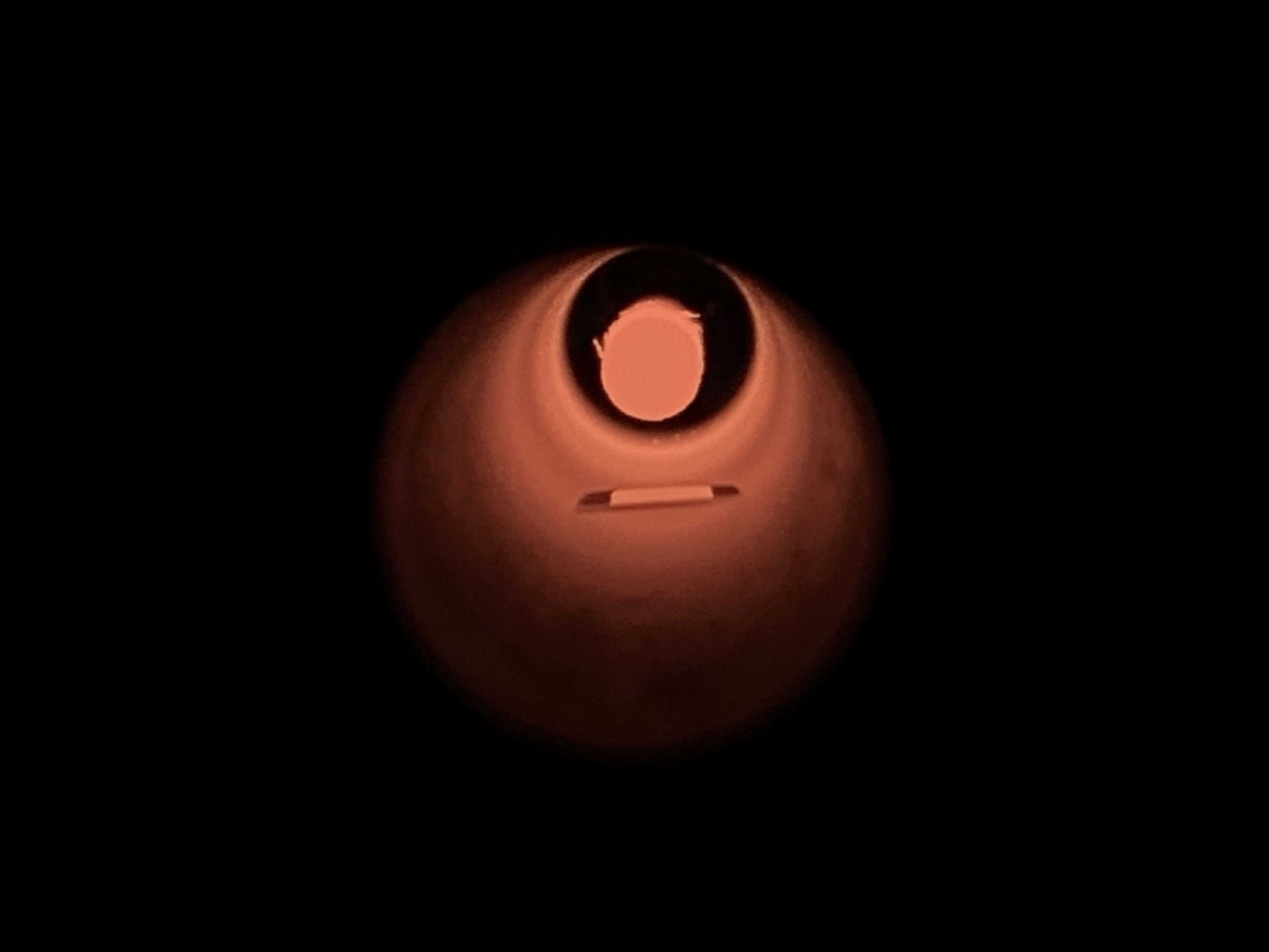
A Die inside of the tube furnace at 1200°C growing an oxide layer
Oxide etch
After growing an oxide layer, it is often necessary to selectively etch it away to expose regions of bare silicon that can be doped or bonded to. This is typically done using hydrofluoric acid or its derivatives. HF is an extremely dangerous acid, as it can easily cause painless yet life-threatening burns. In an abundance of caution, I had access to calcium gluconate gel and an eye wash station. Additionally, measures were taken to contain all potential spills, and no skin was shown at any point when hydrofluoric acid was used.
With this safety warning aside, I used a 2% by weight solution of hydrofluoric acid to etch away thin oxide layers. For thicker oxide layers, I used a special glass etching cream to save time. Etching masks were prepared using copper tape, which I found to stick extremely well to the surface of the die while not reacting adversely with the hydrofluoric acid solution.
The removal of the oxide layer can be easily verified with the observation that water will bead up on the surface of bare silicon but will wet an oxide layer.
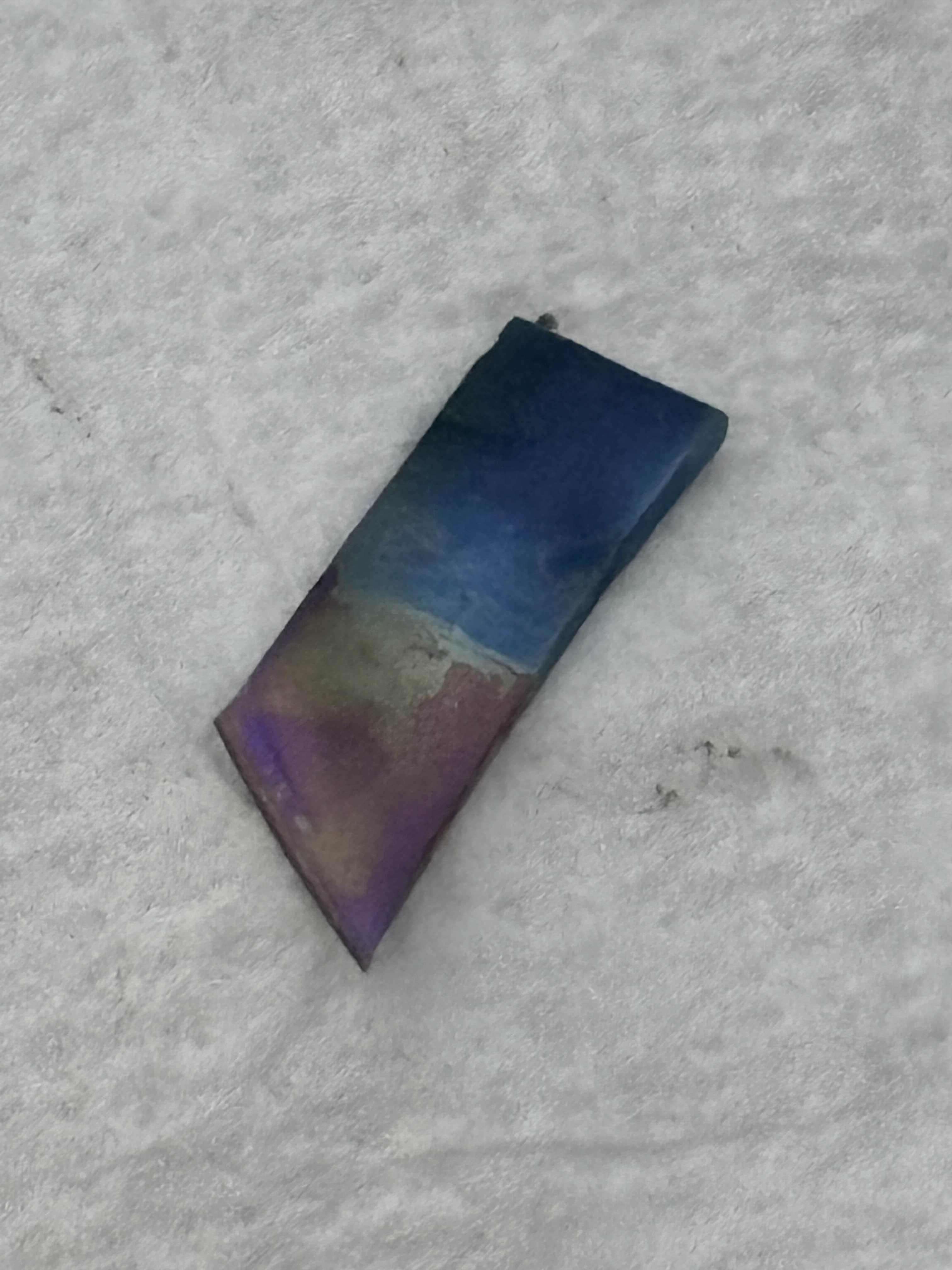
Half of the chip is partially etched, giving it a different color. This is an early test
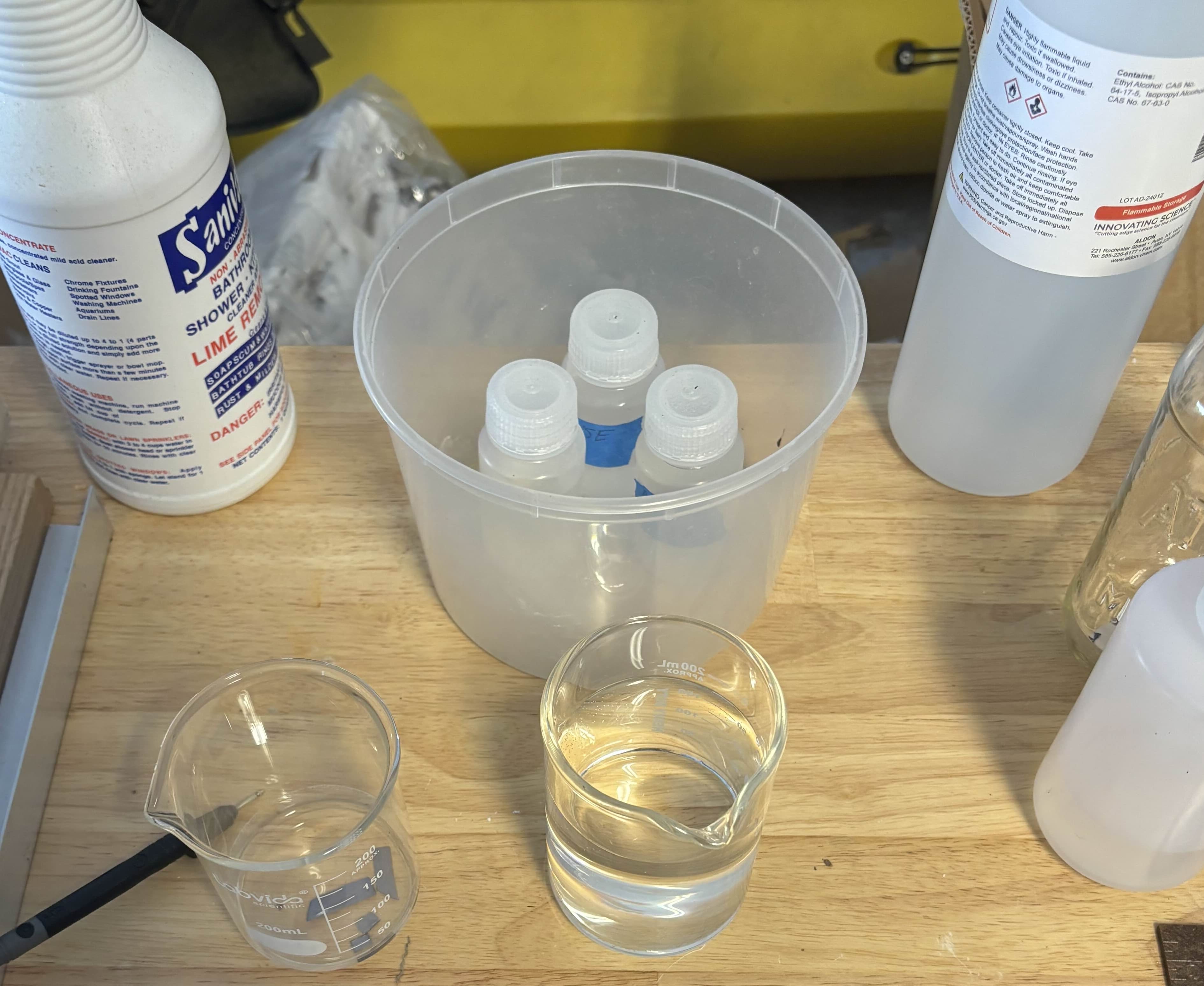
Etching station: One bottle of 2% HF and three bottles of distilled water for washing, all within a spill container. The chips are washed with ethanol and distilled water prior to etching to clean the surface.
Doping
Doping is the process of selectively introducing impurities into silicon to control conductivity. Technically, it introduces new energy levels within the band gap allowing passage for electrons to hop from the valence band to the conductance band.
I did this using thermal diffusion. In the same way that a drop of food coloring in a glass of water will diffuse out, phosphorous atoms on the surface of a silicon die will naturally diffuse into the lattice given time. This process is accelerated by high temperatures, with phosphorous having a maximum solubility in silicon at around 1100°C.
Theoretically, a droplet of phosphoric acid on the surface of the die should be enough for thermal diffusion to occur. While this does work, the phosphoric acid does an extremely poor job of achieving an even doping level. This is because the solution will begin to bubble and splatter as it heats up, creating an uneven coating. Therefore, in industry, spin-on dopants are typically used instead. In my case, I used a solution of tetra-ethylorthosilicate (TEOS) and phosphoric acid, along with ethanol and water to improve viscosity and wetting of the die surface. This solution is a liquid normally, but when spread thinly across the surface of a die, it dries out and forms a silica gel matrix containing phosphate ions. This silica matrix is much more resilient to higher temperatures, and keeps the phosphorous atoms spread evenly across the surface of the die, achieving an even doping level.
Successful doping can be verified using a hot probe test, as well as measuring the resistance of the wafer before and after doping.
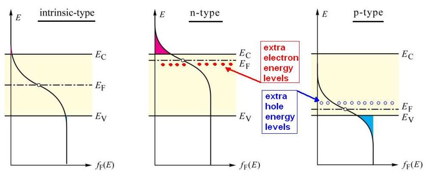
Addition of impurity atoms in a semiconductor creates new energy levels and shifts the fermi energy.
Metallic contacts
Although not listed as an explicit step, it is important to form proper metallic contacts to the surface of the die so that it can be used in a circuit. This is more difficult than you may expect, as not all metals are compatible with silicon. This is because they can form non-ohmic contacts, aka schottkey junctions, which are potential barriers that hinder electron flow.
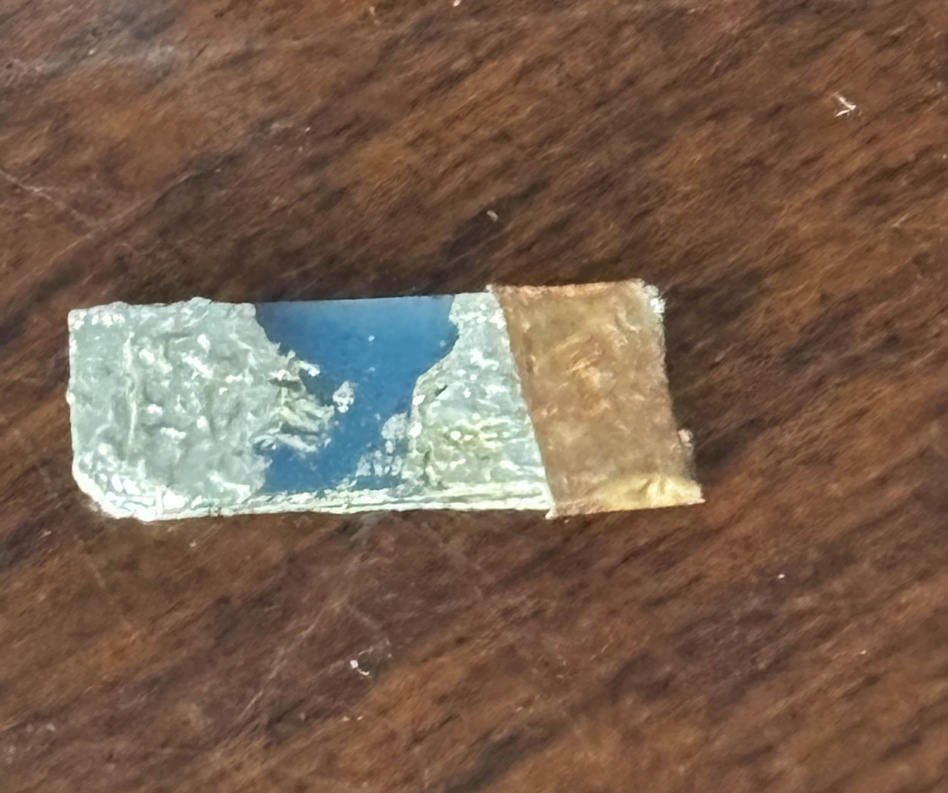
In my work, I spread silver epoxy over the contacts, as silver has a work function relatively similar to silicon which makes it compatible. This silver epoxy was somewhat fragile, so I put a layer of copper tape over it.
Diode Fabrication
I created a diode which was simply a PN junction. First I grew an oxide layer over a silicon die at 1200°C. After taping off half of the chip, I etched away the exposed oxide to the bare silicon. Spin-on dopant was then applied and phosphorus atoms were selectively driven into the exposed half of the die, turning it from P-type to N-type silicon. After etching again and creating metal contacts, the diode was finished.
The activity of the diode was verified using the photoelectric effect. When photons strike a PN junction, they can excite electrons into the conducting band, creating charge carriers. These charge carriers are then able to move across the depletion region and generate small currents, which can be measured with a multimeter. Sure enough, when I placed my diode under bright lights, a small voltage around 50mV was generated.
The finished PN Junction diode