8-Bit Breadboard Computer
Example: Fibonacci Sequence Calculation
As an example, the computer is able to calculate the Fibonacci sequence (0, 1, 2, 3, 5, 8, 13, ...). This program is implemented into the computer as follows:
1) LOAD "0" into register A
2) LOAD "1" into register B
3) ADD A+B, load contents into register C
4) MOVE contents of register C into register A
5) ADD A+B, load contents into register D
6) MOVE contents of register D into register B
7) JUMP to step 3
This program demonstrates data loading into 4 registers and an unconditional jump instruction.
Video Demonstration
[video]
Computer Architecture and Build

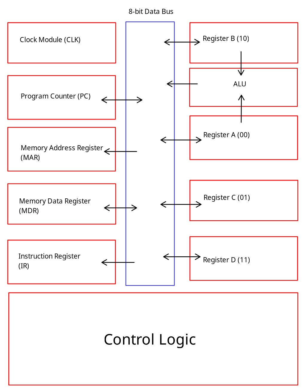
This computer utilizes the von Neumann architecture where programs are stored in the same memory as data. It contains a clock module, program counter, memory address register and RAM module, memory data register (MDR), instruction register (IR), and 4 general purpose registers labeled A through D. Finally, an EEPROM control logic module is used to drive the numerous CPU control signals to execute each microinstruction.
Overall, this computer runs on 4.5 volts from a benchtop DC power supply, drawing roughly 1.5 amps when all lights are on.
Clock Module (CLK)
The clock module is driven by a 555 timer running in either the astable or monostable mode. The clock frequency can be adjusted using a potentiometer.
Program Counter (PC)
The PC is a module in the computer that stores the next step in the program to be executed. It counts between 0 and 16, meaning that a program can contain a maximum of 16 steps.
It is built off a pair of 74LS161 synchronous 4-bit binary counters, although in practice, the computer only utilizes the first 4 bits of the counter.
This module supports three control signals: Clear, Enable counting, and Load data. Clearing wipes the contents of the counter, resetting it back to 0, while enable counting allows for the counter to count forward with each clock cycle. Finally, Load data allows the counter to load a value from the data bus, effectively functioning as a goto flag. Counting is done on the rising edge of each clock cycle.
Memory Address Register (MAR)
The MAR is a register used to store RAM addresses. It reads a memory address from the data bus and feeds it to the RAM module. The design of this register is essentially the same as every other register, using a 74LS245 tri-state buffer to connect to the bus, and a pair of 74LS175 4-bit D-flip flops to store 8-bits of data in total.
This module has 2 control signals: Clear and MAR In. Clearing wipes the contents of the register, while MAR in loads the contents of the bus into the MAR.
Memory Data Register
The MDR is a register used to store RAM data. After a memory address is provided to the RAM module, the output data is loaded into the MDR upon the next clock cycle. This register is designed the same as every other register in the computer.
This module has 3 control signals: Clear, MDR In, and MDR Out. Clear wipes the contents of the register, MDR In loads data in from the bus, allowing programs to write data to memory, and MDR Out outputs the contents to the bus.
Instruction Register (IR)
The IR is a register that holds the current instruction being executed. Instructions are 8-bit words divided into a 4-bit Opcode and a 4-bit parameter. The IR is able to load instructions from the data bus, and output directly to the control logic module.
It has only two control signals: Clear and IR In. Clearing wipes the module and IR In loads the contents of the bus into the register.
Registers A-B (Ra, Rb, Rc, Rd)
The computer contains four general purpose 8-bit registers for programs to use. The first two, A and B, directly load into the ALU, but the others, C and D, are independent of each other. Each register is capable of bidirectional communication with the bus, and is controlled by three control signals: Clear, Register In, Register Out.
Arithmetic Logic Unit (ALU)
The ALU is a made of a pair of 74LS83 4-bit binary full adders, with a carry flag being activated if the sum overflows the 8 available bits. It is controlled by two control signals: Clear and Sum Out.
Control Logic
The control logic is the heart of the computer, deciding which control flags to activate for each microinstruction. It is built out of 4 8-bit AT28C64 EEPROM IC's with 14 bit addresses.
Each 14 bit EEPROM address is broken down into 4-bit sections. The first 4 bits is the instruction Opcode, followed by the 4-bit parameters, and finally by a 4-bit microinstruction counter output. The last 2 bits are unused.
The 4-bit microinstruction counter allows for 16 microinstructions per instruction, where each microinstruction is a set of control signals to set high during each clock cycle.
The EEPROM output is directly linked to the control signals of the CPU, allowing the control logic to decide which signals need to be set high for each input.
Open Source Schematics
I am currently working on a set of circuit schematics for this computer, along with the exact BOM used. These should be coming out in a few months, and will be freely available here.